
Microsoft Maia 200 – AI chip with 216 GB of HBM3e, 750 W TDP and 10 petaflops
02.02.26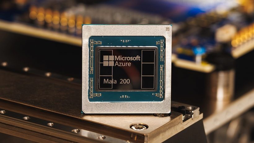
Microsoft officially announced its Azure Maia 200 server-based AI accelerator, the second-generation chip in the Maia line, designed specifically for AI inference. The company calls it the most efficient inference system in its history, claiming approximately 30% higher performance per dollar compared to the Maia 100.
Architecture and Process Technology
The Maia 200 is manufactured on TSMC’s 3nm process and contains approximately 140 billion transistors. According to Microsoft, the chip delivers up to 10 petaflops of FP4 performance, approximately three times higher than Amazon Trainium3. The accelerator is equipped with 216 GB of HBM3e memory with 7 TB/s of throughput and 272 MB of on-chip SRAM.
Memory Approach
The company placed special emphasis on the memory architecture. The integrated SRAM is divided into Cluster-level SRAM (CSRAM) and Tile-level SRAM (TSRAM). This division allows for more efficient load balancing between fast local memory and HBM, which positively impacts stability and power efficiency when working with FP4 and FP8 formats, which are key for modern inference models.
Power Consumption and Efficiency
Despite the Maia 200’s stated TDP being 50% higher than that of the Maia 100, Microsoft claims overall power efficiency has increased. For comparison, the Nvidia Blackwell B300 Ultra has a TDP of approximately 1400W, while the Maia 200 operates at 750W. Meanwhile, the Maia 100, nominally rated for 700W, consumed around 500W in practice.
Competitor Comparison and Positioning
The company does not directly compare the Maia 200 with Nvidia solutions, as the chip is not sold to third-party customers, and Nvidia’s software ecosystem remains significantly more mature. However, from a power efficiency perspective, Microsoft’s own solution appears compelling—especially amid growing attention to the environmental impact of AI and data center power consumption.
Deployment in Azure Datacenters
Maia 200 accelerators are already operational in the Azure US Central datacenter. Microsoft plans to expand their deployment to US West 3 (Phoenix, Arizona) and other locations soon. The chips will be part of a hybrid infrastructure where Maia 200 accelerators will operate alongside other Azure SI accelerators.
Don't miss interesting news
Subscribe to our channels and read announcements of high-tech news, tes
Oppo A6 Pro smartphone review: ambitious

Creating new mid-range smartphones is no easy task. Manufacturers have to balance performance, camera capabilities, displays, and the overall cost impact of each component. How the new Oppo A6 Pro balances these factors is discussed in our review.
Oppo Reno 15 5G smartphone review: confident

The Oppo Reno15 smartphone emphasizes design, a high-quality display, versatile cameras, and good battery life. Let’s take a closer look.
Microsoft adds image support to Notepad Microsoft update

Microsoft continues to expand the capabilities of the updated Notepad in Windows 11. The next step may be image support
ASUS and Acer stop selling laptops and operating websites in Germany due to Nokia’s victory in court Acer Asus court of law Nokia world events

In 2025, Nokia filed parallel lawsuits against Acer, Asus, and TV manufacturer Hisense at the Munich Regional Court and the Unified Patent Court.